Introduction
Thinklaser Limited has long supported electronics manufacturers with innovative laser marking solutions, especially for integrated circuit (IC) devices requiring permanent identification. Our legacy work in laser marking IC devices stands as a benchmark in the industry, reflecting our commitment to quality and precision.
Client Background and Initial Challenges
In the early 2000s, a global electronics company sought Thinklaser’s expertise to address challenges in identifying and tracking their IC devices. They needed a solution that would provide a unique, durable, and high-contrast mark on each device, ensuring protection against counterfeiting and easy traceability in a fast-paced production environment. Traditional marking methods fell short, unable to deliver the required durability or precision on such small components.
Solution Overview
Thinklaser’s legacy approach involved pioneering fibre laser technology, customised for laser marking IC devices to achieve high-resolution, non-intrusive marking. These laser systems produced clear and durable marks, resilient to extreme temperatures, handling, and environmental exposure – ideal for electronic components used in demanding applications.
Key features of the Thinklaser solution included:
- High-Precision Marking: The laser created fine, intricate markings, such as serial numbers, logos, or batch codes, without damaging the ICs.
- Permanent Durability: Unlike ink or etching, the laser marks were impervious to wear, providing lifetime identification.
- Compact Marking for Small Surface Areas: Thinklaser’s solution addressed the unique space limitations of IC devices, producing clear, readable marks even on very small surfaces.
Real Life Application: Laser Marking IC Devices – IBM
Back in the day, when a computer processor actually had value, manufacturers played with the idea of being able to identify their products. This followed a court case, in America, where thieves walked out of court because the prosecution were unable to prove that product (devices) found on the arrested individuals belonged to their client, the manufacturer. IBM led the field with a programme that had them facilitate all their manufacturing sites worldwide with laser marking, in order to customise their product for future reference. The programme included laser marking the outside, but also logging ID numbers within the chips reference library.
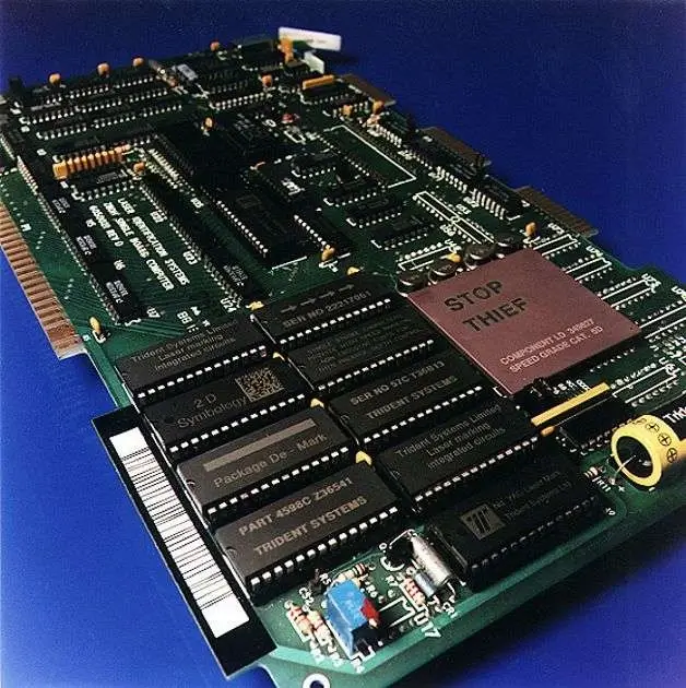
The photo shows a number of different chipsets, all laser marked with a variety of identifying information. ND:YAG was used to mark the selection of plastic and ceramic based components. Some complications arose from marking too deep, but these were resolved quickly. The detail required at this level is quite remarkable, but the laser marking does not affect bonding wires yet, is of course, permanent.
Due to the quantity required in each manufacturing batch, the M series was built with a tray to tray transfer facility (Jedec trays were used to transport most of the devices being used). The scan field was able to process approx. half of the tray in one sequence; the tray would then be indexed so that the remaining devices could be processed. The trays were then sent to an off load station, where non tray based devices were marked, we provided a tube to tube facility, based on gravity feed through the laser marking area.
Nd:YAG laser marking was used back then. Fibre technology is more likely to be used today as it can cope with both materials very well.
Legacy Impact and Long-Term Benefits
Over two decades, our laser marking IC devices solution has demonstrated significant long-term value:
- Enhanced Traceability: The laser markings enabled the client to accurately track each IC throughout its manufacturing process and lifecycle.
- Counterfeit Prevention: Permanent, unique identifiers provided a strong deterrent to counterfeiting, improving brand security.
- Increased Efficiency: The automated, high-speed marking process seamlessly integrated with high-volume production lines, reducing downtime and operational costs.
Continued Relevance
Thinklaser’s legacy in laser marking IC devices has laid the foundation for current industry standards in protective marking. Many of our early innovations in this field are now regarded as essential features in the electronics manufacturing process. Today, our solutions continue to evolve, with enhanced software integration and improved laser precision, yet they remain rooted in the principles established by this foundational project.
Conclusion
Thinklaser Limited’s legacy work in laser marking IC devices set a new standard for protective identification in the electronics industry. Our pioneering approach has not only served our clients well over the years but also shaped industry expectations for quality, durability, and security in electronic component marking.
If you would like further information on this application, or any other application, please request a call back or, talk to one of our laser marking specialists by going to our contact page – link below.
Contact Us for Laser Engraving, Marking & Cutting Advice (thinklaser.theprogressteam.com/)
